为奥特斯及其客户实现可持续创新
电子工业的特点是持续快速发展并且经常有技术突破。奥特斯的客户是有各行各业的一流企业。他们希望我们的产品和工艺符合高标准,并具有足够的灵活性,以跟上行业快速创新的步伐。
我们重视研发,所以坚持不懈地开发我们的技术,确保客户的想法能尽快落地。自奥特斯成立以来,我们已经证明大胆投入研发必有回报。同时,我们也高度重视可持续发展概念,并利用新技术减少我们集团以及我们的合作伙伴公司的环境足迹。

无论是在技术、业务流程还是实施环境改善方面,从最初的想法到执行,创新都是推动奥特斯前进的动力。我们正在为塑造一个互联互通的未来作出重要的贡献。
Hannes Voraberger, 公司副总裁 研发部
更快、更绿色、更好的互联
我们不遗余力地积极打造未来技术,提供创新解决方案解决客户的技术问题。毕竟,只有这样才能在竞争中先行一步,继续在微电子革命中发挥关键作用,并为解决我们社会面临的重大挑战作出重要贡献。同时,强大的电子系统正推动经济数字化和脱碳进程,为实现低成本、灵活控制各种系统开辟了道路:例如,风力发电厂依靠智能控制才能高效运转。强大的计算机、服务器和移动设备中使用的微芯片也是如此。
奥特斯技术应用于处理器,并实现微芯片与计算机中其它必备元件之间的通信。
我们的印制电路板(PCB)和半导体封装载板不仅可以确保快速处理数据,还通过进一步微型化真正地大幅降低能耗。奥特斯在环境责任方面以严格的标准要求自己以及我们的供应商,始终确保我们的技术进步不以牺牲环境为代价。我们以全局思维看待未来的世界。我们秉承全面的可持续生产理念,不断升级完善,促使我们使用更环保的材料和更节能的基础设施。我们积极主动地确保我们拥有一个不断进步并适于居住和生活的未来。
研发助力
为了保持我们在技术和环保责任方面的领先地位,我们将10%的收入投入新产品和新工艺的研发。目前,这相当于每年投入约1.554 亿欧元。我们在奥地利的工厂从这项投资中受益匪浅,已经有一大批先进的技术准备投产。

奥特斯 在高科技印制电路板(PCB)和半导体封装载板的生产制造方面拥有800多项专利。这些创新产品和技术是我们收入的重要贡献者,它们经过数年的研发,在投入市场三年后,为我们带来25,9%的收入。

新研发中心:奥地利和欧洲其它地区的高科技

未来几年,奥特斯计划投资5亿欧元在利奥本新建一个研发中心,该研发中心将雇佣700名新员工。
到2025年,奥特斯位于利奥本的总部将新建一个研发中心和配套生产工厂。新大楼的建设将耗资约5亿欧元,研发中心和生产工厂的面积超过1万平方米。这将总共创造700个新的工作岗位。
新的研发中心标志着奥特斯集团对持续技术开发和利奥本生产基地的承诺。这里将见证许多新产品和新想法的诞生,继续为奥特斯走向光明的未来保驾护航。新的研发中心还将为利奥本带来半导体封装载板生产方面的专业知识,使奥地利能够再次吸引高科技电子和半导体行业的精英人才。
这是欧洲地区的一个灯塔项目,因为它将是欧洲大陆一个半导体封装载板生产工厂。目前,半导体封装载板及移动设备事业部占奥特斯总销售额的近四分之三,随着利奥本生产基地的扩张,该事业部的贡献将更加明显。


数据、数据、数据
电子工业蓬勃发展的核心是数据革命,近年来,数据革命彻底改变了行业和我们的日常生活。记录、储存和分析的数据与日俱增,目的是让我们能够尽可能高效地处理流程,以及访问各种各样的在线服务。这些发展需要数据处理系统不仅能耗低还可以高效地传输信号,同时仍然允许高度的复杂性。无论在汽车行业、医疗技术还是半导体生产中,微电子系统的设计者和制造商都可以利用奥特斯的印制电路板(PCB)和半导体封装载板来满足这些要求。
通过持续的技术开发,我们确保电路板在能源消耗和信号传输效率方面处于重要地位。
我们与客户合作开发和优化我们的产品,而且现在是在一个完全数字化的环境中进行协作。
这不仅可以简化改进工作,还更便于实施减少环境影响的措施。我们与我们的供应商和业务合作伙伴都使用这一方法,因此我们可以共同帮助确定整个生产生态系统的优先事务。我们努力以尽可能微型化的微电子系统实现低资源消耗,确保高效处理数据,信号线高速节能。


科学与工业界的合作伙伴
为了保持行业技术的领先地位,我们在地区、国家和国际层面与一些最负盛名的研究机构和行业合作伙伴开展合作。
通过有效利用资源和知识共享,我们能够与这些合作伙伴一起开展创新研发。
学术合作伙伴带来了深入的理论知识和研究成果,而行业合作伙伴则贡献了实践经验和市场知识。这种协同作用使我们能够更快地将研究成果转化为适销对路的产品和解决方案。例如,密切合作意味着可以更快地开发和测试原型。这大大缩短了创新周期。
通过将战略投资与优秀的研究合作伙伴相结合,我们正在巩固我们的技术领先地位,并帮助塑造电子行业的未来。
促进科研:奥特斯项目和合作
作为一家创新型高科技公司,奥特斯是奥地利乃至整个欧洲科研领域的重要一员。高质量的研发工作让我们获得了著名资助项目的资金支持,并有机会与众多国际知名的合作伙伴合作。欲了解更多信息,请点击此处:

IPCEI 微电子和通信技术 (IPCEI ME/CT)
IPCEI ME/CT 涉及从材料和工具到芯片设计和制造工艺的整个价值链上的微电子和通信技术研发项目。
这些项目旨在通过以下方式实现数字化和绿色转型
- 创造创新的微电子和通信解决方案,以及and
- 开发节能、节约资源的电子系统和制造方法。
它们将推动重要行业领域的技术进步,包括通信(5G 和 6G)、自动驾驶、人工智能和量子计算。它们还将通过促进能源的可持续生产、分配和使用,积极支持企业实现绿色转型。
IPCEI ME/CT 通过支持微电子领域的研究和创新,继承和补充了已经成功完成的首届 IPCEI。
该项目由十四个会员国共同筹备和宣布: 奥地利、捷克、芬兰、法国、德国、希腊、爱尔兰、意大利、马耳他、荷兰、波兰、罗马尼亚、斯洛伐克和西班牙。
奥特斯 – IPCEI ME/CT 的一员
奥特斯的目标是加强其在价值创造链中的地位,并通过建立先进集成电路基板和封装技术的研发线、原型和小批量生产线,进入新的、高要求的专业领域。新设施将打造一个世界级的有机集成电路基板和高度集成模块能力中心。
通过该项目,奥特斯将实现与 “思考”(THINK)工作流相关的以下总体目标 — 半导体技术、智能制造。
- 模拟未来
虚拟开发和系统理解,致力于欧洲技术先进地位 - 微型化
2nm 节点处理器的基底级功能 - 柔性制造
加快开发周期,实现小批量生产 - 模具整合
提高系统能效
奥特斯的工作重点是打造和加强智能化和可持续的
- 先进扇出、集成电路基板和封装技术的研发线,目标是将新一代集成电路基板的布线密度提高 6 倍。
- 集成电路基板和封装技术的原型和小批量生产线。
- 先进扇出、集成电路基板和封装技术的工业开发能力中心,利用这些能力与不同的合作伙伴进行互动和合作。
奥特斯 IPCEI ME/CT 外溢活动包括以下内容:
产业合作与研究合作
在 IPCEI ME/CT 的推动下,奥特斯将支持和加强欧洲价值链上的开发活动,并与大学和研究与技术组织合作。通过这些活动,我们将为欧洲带来积极的溢出效应。
加强教育和人才培养,共享专业知识
奥特斯将促进大学在科学、技术、工程和数学领域的参与,并将知识提供给合作伙伴(中小型企业、大学和研究与技术组织)。
![]() Horizon Europe – 人工智能驱动的微电子再可靠性 (MIRELAI)
Horizon Europe – 人工智能驱动的微电子再可靠性 (MIRELAI)
MIRELAI 是一个由欧盟资助的工业博士网络,旨在应对与微电子元件生产相关的可靠性、可持续性和验证工作方面的挑战,提高欧洲的创新能力和市场竞争力。
为实现这一目标,该项目招募了 13 名博士候选人(DCs),以研究降解物理学,减少整个电子元件和系统价值链的测试和验证工作,同时为下一代工程师提供宝贵的技能。
![]()
SHIFT 是一个由欧洲资助的项目,其目标是开发一种创新的收发器原型,使未来一代移动设备能够高效利用 100GHz 以上的宽频谱。
SHIFT 将为新型 SiGe BiCMOS 技术和集成概念开发一个技术设计平台。该平台可用于设计超高频(电信、医疗、仪器仪表、智能移动、机器人、工业)的商用 MMIC,最高频率可达 200GHz。
概念:
- 应用(系统规格、TX/RX、电路)
- 设计 B55X 电路设计、功率放大器设计、射频插层设计
- 发射机/接收机集成(射频集成电路/PCB)
- TRX 系统的开发和验证
![]()
CHIPS JU – 异构集成实现连接性和可持续性 (HiConnects)
HiConnects 是一个由欧洲资助的项目,其目标是开发创新的面板级封装技术,在嵌入式基础上高度集成先进的异构光子和射频元件。
为未来的集成电路基板开发结构化和集成工艺,并对合适的工艺和计量设备开发进行无损检测。
开发具有更高带宽和更低能耗的下一代智能网卡和交换机平台的光学集成。
为 77 GhZ 和 144 GhZ 汽车雷达开发集成射频元件。
MICROELEctronic 2 market – InnoPower
该项目是嵌入式领域的一项发展,即把半导体元件集成到印刷电路板中(“工艺流程中心核心嵌入”)。
在这种具体情况下,它涉及到直流/直流转换器的生产,该转换器可将直流输入电压(DC)转换为直流输出电压(DC = 直流)。为了生产这种直流/直流转换器,需要将驱动器和 SFET(半导体场效应晶体管)元件集成到印刷电路板上的一小块区域内,以实现可用于 “人工智能 ”领域的封装。通过集成半导体元件,可以显著缩小 DC/DC 转换器的尺寸。与 “最先进 ”的产品相比,体积可缩小 50%以上。
创新营 M – DeCarb
从科学到行动,增强企业实现零碳的能力
由 FFG(Österreichische Forschungsförderungsgesellschaft )资助的 DeCarb 项目的目标是,通过在脱碳方面的专业技术领先优势,增强企业的竞争力并确保其位置。此外,还建立了一个由气候先锋组成的最佳实践社区,他们发挥着倍增器的作用。
![]()
Horizon Europe – 超动态光子开关和收发器的封装 (PUNCH)
封装新型 Ultra-dyNamiC pHotonic 交换机和收发器,以便集成到 5G 无线接入网络和数据中心子系统中。
新型光交换机可以加快数据网络骨干网的速度。欧盟资助的 PUNCH 项目将开发一种新的光交换解决方案,以满足多项工业要求,包括保证服务质量的可靠和低延迟通信、减少网络拥塞(以及数据丢失或延迟)、降低功耗和减少传输接口的成本。
为此,PUNCH 将开发新型光子元件和相应的接口电子设备,建立可扩展的集成和光子封装流程及 ICS,并制造不同的原型,在工业 5G 和数据中心测试平台上进行演示和验证。
![]()
CHIPS JU – 欧洲绿色电子生态系统 (EECONE)
EECONE – 欧洲绿色电子生态系统是欧盟芯片项目,有来自欧洲各国的 40 多个合作伙伴参与。该项目的目标是找到减少电子垃圾和提高整个电子行业可持续性的方法。
在该项目中,奥特斯正在开发一套生命周期评估工具以及减少印刷电路板制造环境足迹的概念。
SFG – 多功能工具 Infinity C+
由 SFG 资助的 “Multiwet Tool Infinity C+”项目是关于一种灵活的机器,可在一台机器上实现多种湿化学工艺。
由于多种原因,这种灵活性是将机器用于研发应用的上佳选择。
设备的配置可实现多达六种不同的工艺。这些工艺通常在非常大的水平或垂直生产线上实现,但为了节省洁净室设施的空间,在该设备上以压缩的方式实现。
单室加工优化了可持续发展,并保护了环境,因为在冲洗过程中化学品和水的消耗量降到了最低。
蚀刻薄金属层以及显影和剥离感光层等工艺对奥特斯在欧洲的集成电路基板技术的发展至关重要。
独特的系统使奥特斯和客户能够深入了解半导体工艺世界
作为其研发线的一部分,奥特斯已决定从 Evatec 购买物理薄膜系统 “Clusterline 600”。这项新技术用于开发新一代集成电路基板、新颖的嵌入概念、异构集成、高级封装和 FO-PLP(扇出-面板级封装)。
![]() 基于模块化、智能化和高度集成的宽带隙电力电子模块的高效可靠的电动传动系统
基于模块化、智能化和高度集成的宽带隙电力电子模块的高效可靠的电动传动系统
该项目重点开发最先进、集成和可靠的宽带隙(WBG)技术,包括用于电动汽车和充电设施的高能效、可靠电力电子设备。
这将推动智能移动出行的发展,对整个价值链中各个层面产生重大影响。HiEFFICIENT合作伙伴制定了雄心勃勃的目标,不仅要提高市场对WBG半导体的接受度,还要实现最大的效益。
![]()
D波段无线电5G网络技术
DRAGON项目将使用D波段(130-174.8 GHz)1无线电频谱来克服目前E波段无线回程解决方案的局限性,以实现一个合适的小尺寸、大容量无线电解决方案。这对于该技术的大规模部署至关重要,因为它能够以低成本实现回程系统达到光学系统的速度。DRAGON为新的半导体、天线和封装技术以及由此产生的硬件设备进入市场提供了巨大前景,并创造了新的商机。
联系人

我们随时为您效劳!
如果您想了解更多有关我们出色的产品、技术和解决方案的信息,我们的专家随时乐意为您提供帮助。
您可能还对这些主题感兴趣

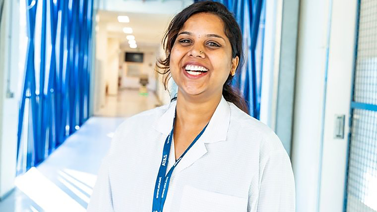
AT&S owes its success to high-tech and, above all, to the committed employees worldwide. Our category "The people behind AT&S" presents these inspiring colleagues.
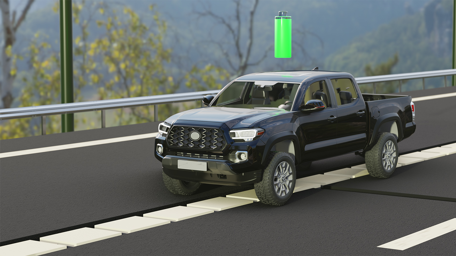
Range remains a perennial issue in the discussion about e-mobility. In the future, roads could charge vehicles using induction - but the technology is only at the testing stage.