利用嵌入式组件封装(ECP®) 技术实现微型化
非常紧凑的印制电路板
我们采用ECP®技术的印制电路板是我们多年来致力于微型化开发工作的结晶。通过在电路板中“埋嵌”元件,我们创建了第三个功能层:这样电路板内层也有了宝贵的空间,而不仅只限于顶层和底层。这样的电路板比相同尺寸的传统电路板可以实现的功能更多。我们的ECP®印制电路板被用于各种高科技应用,从医疗技术到消费类电子产品。
ECP®技术是医疗技术和消费电子等领域实现微型化的核心驱动力。 该技术助力打造更轻薄、更小型化的设备,同时确保性能表现不受折损。
嵌入式组件封装(ECP®)技术的优点
- 为集成元件提供优秀的保护和良好的散热性,非常可靠。
- 外形薄有助于余热极快消散 – 这一点对于许多电力电子控制应用非常重要。
- 无可比拟的微型化程度,使印制电路板可以实现新的、更小的造型。
- 系统微型化使信号路径变短,损耗降到极低。
激光技术实现高精度
为了将元件放置在印制电路板内层中,我们使用先进的激光技术将内层中目标区域的材料去除。然后将这些元件置于凹槽和层中,不留一点空隙,同时对嵌入的元件进行良好的保护。然后通过激光钻孔建立连接。
奥特斯使用新的激光技术,用PCB(印制电路板)扇区工具制造出非常紧凑的电路。
存取系统、植入元件和平板电脑
ECP®印制电路板在电子工业的各个领域都有着重要的应用。它们轻薄的设计使其成为超薄智能手机和平板电脑的理想选择。微型通讯模块也可以封装在智能笔和其它非常规的外形设备中,为消费类电子产品开辟了新天地。
在智能手机领域,这些小小的电路板可以实现体积更大、电量更持久的电池应用。使用ECP®技术的充电器可以加快电池充电速度。电子门禁系统、数据中心、智能工厂和医疗技术都受益于这些PCB产品更小的系统尺寸和更高的可靠性。
,On,Hands")


技术详情

| Product Characteristics | Specifications |
|---|---|
| Layer count | 4 to 14 layers |
| Embedded core layer count | 2 or 4 layers |
| Copper nominal thickness | PP: 12 to 35 µm |
| Die to package ratio | standard max. 50% |
| Component thickness | 55 to 500 µm |
联系人

如果您想进一步了解我们令人兴奋的产品、技术和解决方案,我们的专家随时乐意为您提供帮助。
您可能还对这些主题感兴趣
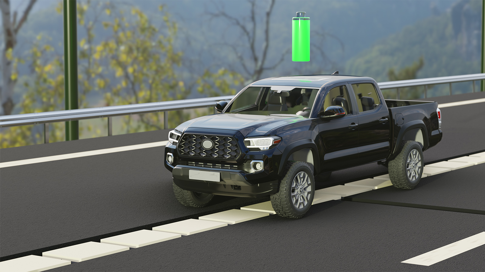
Range remains a perennial issue in the discussion about e-mobility. In the future, roads could charge vehicles using induction - but the technology is only at the testing stage.
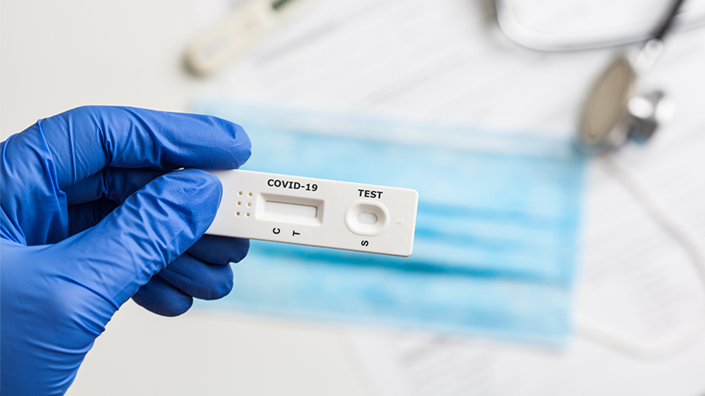
There are different ways to prove that someone has been infected with the coronavirus. Currently, three methods are predominantly used. However, researchers are already working on new procedures in laboratories which should enable faster results or easier delivery. AT&S printed circuit boards play an important role in these processes.

Thanks to flexible electronics and progress in sensor technology, clothing can carry out medical tasks.